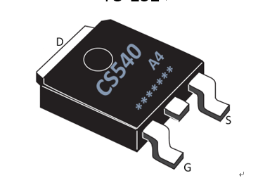
General Description: The CS540A4 uses advanced trench technology and design to provide excellent RDS(ON) with low gate charge. It can be used in a wide variety of applications. The package form is TO-252, which accords with the RoHS standard.
Features: Fast Switching Low Gate Charge and Rdson Low Reverse transfer capacitances 100% Single Pulse avalanche energy Test
Applications: Power switching application Hard switched and high frequency circuits Uninterruptible power supply | 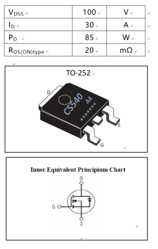 |
Absolute(Tc= 25℃ unless otherwise specified):
Symbol | Parameter | Rating | Units |
VDSS | Drain-to-Source Voltage | 100 | V |
ID | Continuous Drain Current | 30 | A |
| Continuous Drain Current TC = 100 °C | 21 | A |
IDM | Pulsed Drain Current | 120 | A |
VGS | Gate-to-Source Voltage | ±20 | V |
EAS a2 | Single Pulse Avalanche Energy | 260 | mJ |
EAR a1 | Avalanche Energy ,Repetitive | 35 | mJ |
IAR a1 | Avalanche Current | 8 | A |
dv/dt a3 | Peak Diode Recovery dv/dt | 5.0 | V/ns |
PD | Power Dissipation | 85 | W |
TJ,Tstg | Operating Junction and Storage Temperature Range | 175,–55 to 175 | ℃ |
TL | Maximum Temperature for Soldering | 300 | ℃ |
Electrical Characteristics(Tc= 25℃ unless otherwise specified):
OFF Characteristics |
|
|
|
|
|
|
Symbol | Parameter | Test Conditions | Rating | Units |
|
|
|
|
| Min. | Typ. | Max. |
|
VDSS | Drain to Source Breakdown Voltage | VGS=0V, ID=250µA | 100 | -- | -- | V |
ΔBVDSS/ΔTJ | Bvdss Temperature Coefficient | ID=250uA,Reference25℃ | -- | 0.1 | -- | V/℃ |
IDSS | Drain to Source Leakage Current | VDS=100V,VGS=0V,Ta=25℃ | -- | -- | 1 | µA |
|
| VDS=80V,VGS= 0V,Ta=125℃ | -- | -- | 250 |
|
IGSS(F) | Gate to Source Forward Leakage | VGS=+20V | -- | -- | 1 | µA |
IGSS(R) | Gate to Source Reverse Leakage | VGS=-20V | -- | -- | -1 | µA |
ON Characteristics |
|
|
|
|
|
|
Symbol | Parameter | Test Conditions | Rating | Units |
|
|
|
|
| Min. | Typ. | Max. |
|
RDS(ON) | Drain-to-Source On-Resistance | VGS=10V,ID=10A | -- | 20 | 30 | mΩ |
VGS(TH) | Gate Threshold Voltage | VDS = VGS, ID = 250µA | 1.0 | -- | 3.0 | V |
Pulse width tp≤380µs,δ≤2% |
|
|
|
|
|
|
Dynamic Characteristics |
|
|
|
|
|
|
Symbol | Parameter | Test Conditions | Rating | Units |
|
|
|
|
| Min. | Typ. | Max. |
|
gfs | Forward Transconductance | VDS=5V, ID =10.0A | 8.0 | -- | -- | S |
Ciss | Input Capacitance | VGS=0V,VDS=50V f=1.0MHz | -- | 2000 | -- | pF |
Coss | Output Capacitance |
| -- | 300 | -- |
|
Crss | Reverse Transfer Capacitance |
| -- | 250 | -- |
|
Resistive Switching Characteristics |
|
|
|
|
|
|
Symbol | Parameter | Test Conditions | Rating | Units |
|
|
|
|
| Min. | Typ. | Max. |
|
td(ON) | Turn-on Delay Time | ID=15A,VDD=50V VGS=10V,RG=3.0Ω | -- | 10 | -- | ns |
tr | Rise Time |
| -- | 10 | -- |
|
td(OFF) | Turn-Off Delay Time |
| -- | 38 | -- |
|
tf | Fall Time |
| -- | 14 | -- |
|
Qg | Total Gate Charge | ID=15A,VDD=50V VGS=10V | -- | 45 | -- | nC |
Qgs | Gate to Source Charge |
| -- | 12 | -- |
|
Qgd | Gate to Drain (“Miller”)Charge |
| -- | 18 | -- |
|
Source-Drain Diode Characteristics |
|
|
|
|
|
|
Symbol | Parameter | Test Conditions | Rating | Units |
|
|
|
|
| Min. | Typ. | Max. |
|
IS | Continuous Source Current (Body Diode) |
| -- | -- | 30 | A |
ISM | Maximum Pulsed Current (Body Diode) |
| -- | -- | 120 | A |
VSD | Diode Forward Voltage | IS=30A,VGS=0V | -- | -- | 1.5 | V |
trr | Reverse Recovery Time | IS=30A,Tj = 25°C dIF/dt=100A/us,VGS=0V | -- | 66 | -- | ns |
Qrr | Reverse Recovery Charge |
| -- | 130 | -- | nC |
Pulse width tp≤380µs,δ≤2% |
|
|
|
|
|
|
Symbol | Parameter | Typ. | Units |
RθJc | Junction-to-Case | 1.8 | ℃/W |
a1:Repetitive rating; pulse width limited by maximum junction temperature
a2:EAS condition : Tj=25℃,VDD=40V,VG=10V,L=0.5mH,Rg=25Ω
a3:ISD =30A,di/dt ≤100A/us,VDD≤BVDS, Start TJ=25℃

Company:Wuxi Guang Lei electronic technology co., LTD
TEL:13961734102 Mr.yuan