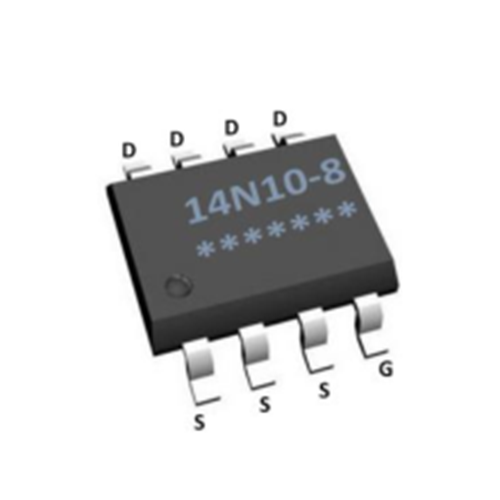
General Description: The GL14N10-8 uses advanced trench technology and design to provide excellent RDS(ON) with low gate charge. It can be used in a wide variety of applications. The package form is SOP-8, which accords with the RoHS standard.
Features: RDS(ON) <12mΩ @ VGS=10V (Typ9.9mΩ) High density cell design for ultra low Rdson Fully characterized avalanche voltage and current Excellent package for good heat dissipation
Applications: Power switching application Hard switched and high frequency circuits Uninterruptible power supply | 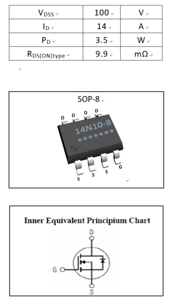 |
Absolute(Tc= 25℃ unless otherwise specified):
Symbol | Parameter | Rating | Units |
VDSS | Drain-to-Source Voltage | 100 | V |
ID | Continuous Drain Current | 14 | A |
IDM | Pulsed Drain Current | 56 | A |
VGS | Gate-to-Source Voltage | ±20 | V |
PD | Power Dissipation | 3.5 | W |
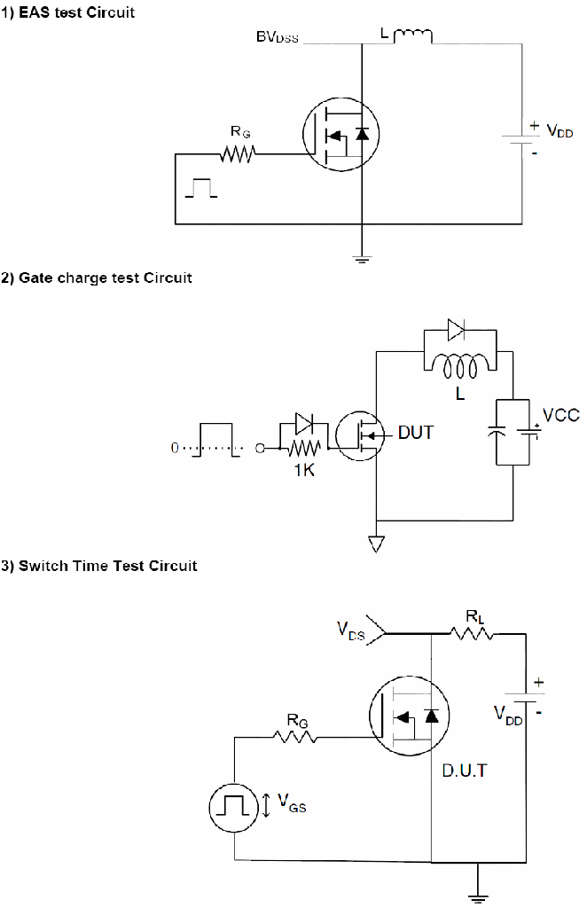
EAS | Single pulse avalanche energya5 | 152 | mJ |
TJ,Tstg | Operating Junction and Storage Temperature Range | 150,–55 to 150 | ℃ |
Electrical Characteristics(Tc= 25℃ unless otherwise specified):
OFF Characteristics |
|
|
|
|
|
|
Symbol | Parameter | Test Conditions | Rating | Units |
|
|
|
|
| Min. | Typ. | Max. |
|
VDSS | Drain to Source Breakdown Voltage | VGS=0V, ID=250µA | 100 | -- | -- | V |
IDSS | Drain to Source Leakage Current | VDS=100V, VGS= 0V,Ta=25℃ | -- | -- | 1.0 | µA |
IGSS(F) | Gate to Source Forward Leakage | VGS=+20V | -- | -- | 0.1 | µA |
IGSS(R) | Gate to Source Reverse Leakage | VGS=-20V | -- | -- | -0.1 | µA |
ON Characteristicsa3 |
|
|
|
|
|
|
Symbol | Parameter | Test Conditions | Rating | Units |
|
|
|
|
| Min. | Typ. | Max. |
|
RDS(ON) | Drain-to-Source On-Resistance | VGS=10V,ID=14A | -- | 9.9 | 12 | mΩ |
VGS(TH) | Gate Threshold Voltage | VDS=VGS,ID=250µA | 1.0 | 1.7 | 2.5 | V |
Pulse width tp≤380µs,δ≤2% |
|
|
|
|
|
|
Dynamic Characteristicsa4 |
|
|
|
|
|
|
Symbol | Parameter | Test Conditions | Rating | Units |
|
|
|
|
| Min. | Typ. | Max. |
|
gfs | Forward Transconductance | VDS=10V,ID=14A | -- | 30 | -- | S |
Ciss | Input Capacitance | VGS=0V,VDS=50V f=1.0MHz | -- | 3050 | -- | pF |
Coss | Output Capacitance |
| -- | 274 | -- |
|
Crss | Reverse Transfer Capacitance |
| -- | 17.8 | -- |
|
Resistive Switching Characteristicsa4 |
|
|
|
|
|
|
Symbol | Parameter | Test Conditions | Rating | Units |
|
|
|
|
| Min. | Typ. | Max. |
|
td(ON) | Turn-on Delay Time | VDD=50V,ID=14A VGS=10V,RG=1.6Ω | -- | 11 | -- | ns |
tr | Rise Time |
| -- | 7.0 | -- |
|
td(OFF) | Turn-Off Delay Time |
| -- | 30 | -- |
|
tf | Fall Time |
| -- | 4.0 | -- |
|
Qg | Total Gate Charge | VDD=50V, ID=14A VGS=10V | -- | 45 | -- | nC |
Qgs | Gate to Source Charge |
| -- | 11.6 | -- |
|
Qgd | Gate to Drain (“Miller”)Charge |
| -- | 6.0 | -- |
|
Source-Drain Diode Characteristics |
|
|
|
|
|
|
Symbol | Parameter | Test Conditions | Rating | Units |
|
|
|
|
| Min. | Typ. | Max. |
|
IS | Continuous Source Current a2(Body Diode) |
| -- | -- | 14 | A |
VSD | Diode Forward Voltagea3 | IS=14A,VGS=0V | -- | -- | 1.2 | V |
Symbol | Parameter | Typ. | Units |
RθJC | Junction-to-Casea2 | 36 | ℃/W |
a1:Repetitive Rating: Pulse width limited by maximum junction temperature.
a2:Surface Mounted on FR4 Board, t≤10sec.
a3:Pulse Test: Pulse Width≤300μs, Duty Cycle≤2%.
a4:Guaranteed by design, not subject to production
a5:EAS condition:Tj=25℃,VDD=50V,VG=10V,L=0.5mH,Rg=25Ω
Test circurt
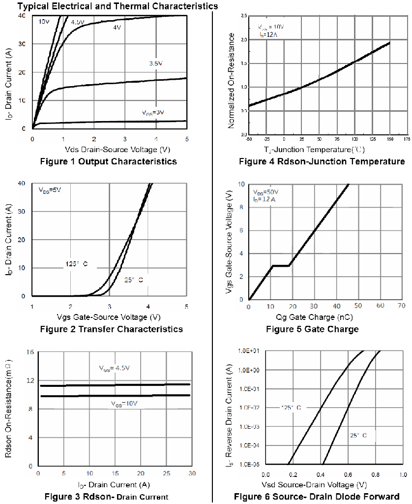
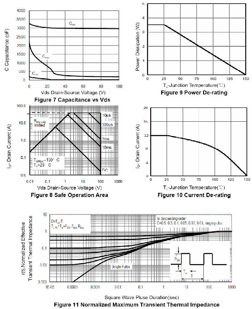
Characteristics Curve:
Company:Wuxi Guang Lei electronic technology co., LTD
TEL:13961734102 Mr.yuan